TeraScale (microarchitecture): Difference between revisions
m →Half-generation update: Task 15: language icon template(s) replaced (1×); |
m Disambiguating links to SUSE (link changed to SUSE S.A.) using DisamAssist. |
||
| (46 intermediate revisions by 29 users not shown) | |||
| Line 1: | Line 1: | ||
{{Short description|Codename for a family of graphics processing unit microarchitectures}} |
|||
'''TeraScale''' is the codename for a family of [[graphics processing unit]] [[microarchitecture]]s developed by [[ATI Technologies]]/[[Advanced Micro Devices|AMD]] and their second [[microarchitecture]] implementing the [[unified shader model]] following ''[[Xenos (graphics chip)|Xenos]]''. TeraScale replaced the old [[Pipeline (computing)|fixed-pipeline]] microarchitectures and competed directly with Nvidia's first unified shader microarchitecture named [[Tesla (microarchitecture)|Tesla]].<ref>{{cite web |url=http://www.tomshardware.com/news/Radeon-HD-6990-DirectX-11-Dual-BIOS-TeraScale-3-dual-GPU,12351.html |title=The TeraScale 3 architecture of the HD 6990 |author=Kevin Parrish |work=[[Tom's Hardware]] |date=March 9, 2011 |accessdate=2015-04-08}}</ref><ref>{{cite web |url=http://s08.idav.ucdavis.edu/houston-amd-terascale.pdf |title=Anatomy of AMD’s TeraScale Graphics Engine |accessdate=2015-04-08}}</ref> |
|||
{{Use mdy dates|date=November 2022}} |
|||
{{More citations needed|date=March 2021}} |
|||
'''TeraScale''' is the codename for a family of [[graphics processing unit]] [[microarchitecture]]s developed by [[ATI Technologies]]/[[Advanced Micro Devices|AMD]] and their second [[microarchitecture]] implementing the [[unified shader model]] following ''[[Xenos (graphics chip)|Xenos]]''. TeraScale replaced the old [[Pipeline (computing)|fixed-pipeline]] microarchitectures and competed directly with Nvidia's first unified shader microarchitecture named [[Tesla (microarchitecture)|Tesla]].<ref>{{cite web |url=http://www.tomshardware.com/news/Radeon-HD-6990-DirectX-11-Dual-BIOS-TeraScale-3-dual-GPU,12351.html |title=The TeraScale 3 architecture of the HD 6990 |author=Kevin Parrish |work=[[Tom's Hardware]] |date=March 9, 2011 |access-date=April 8, 2015}}</ref><ref>{{cite web |url=http://s08.idav.ucdavis.edu/houston-amd-terascale.pdf |url-status=dead |title=Anatomy of AMD's TeraScale Graphics Engine |archive-url=https://web.archive.org/web/20100613174446/http://s08.idav.ucdavis.edu/houston-amd-terascale.pdf |archive-date=June 13, 2010 |access-date=November 21, 2021}}</ref> |
|||
TeraScale was used in [[Radeon HD 2000 |
TeraScale was used in [[Radeon HD 2000 series|Radeon HD 2000]] manufactured in 80 nm and [[65 nm process|65 nm]], [[Radeon HD 3000 series|Radeon HD 3000]] manufactured in 65 nm and 55 nm, [[Radeon HD 4000 series|Radeon HD 4000]] manufactured in 55 nm and 40 nm, [[Radeon HD 5000 series|Radeon HD 5000]] and [[Radeon HD 6000 series|Radeon HD 6000]] manufactured in 40 nm. TeraScale was also used in the [[AMD Accelerated Processing Unit]]s code-named "Brazos", "Llano", "Trinity" and "Richland". TeraScale is even found in some of the succeeding graphics cards brands. |
||
TeraScale is a [[Very long instruction word|VLIW]] [[SIMD]] architecture, while Tesla is a [[Reduced instruction set |
TeraScale is a [[Very long instruction word|VLIW]] [[Single instruction, multiple data|SIMD]] architecture, while Tesla is a [[Reduced instruction set computer|RISC]] SIMD architecture, similar to TeraScale's successor [[Graphics Core Next]]. |
||
TeraScale implements [[HyperZ]].<ref>{{cite web |url=http://xorg.freedesktop.org/wiki/RadeonFeature/ |title=Feature matrix of the free and open-source "Radeon" graphics device driver | |
TeraScale implements [[HyperZ]].<ref>{{cite web |url=http://xorg.freedesktop.org/wiki/RadeonFeature/ |title=Feature matrix of the free and open-source "Radeon" graphics device driver |access-date=July 9, 2014}}</ref> |
||
An LLVM code generator (i.e. a compiler back-end) is available for TeraScale,<ref>{{ |
An LLVM code generator (i.e. a compiler back-end) is available for TeraScale,<ref>{{Cite web|url=https://lists.llvm.org/pipermail/llvm-dev/2012-March/048409.html|title=[LLVMdev] RFC: R600, a new backend for AMD GPUs|first=Tom|last=Stellard|date=March 26, 2012}}</ref> but it seems to be missing in LLVM's matrix.<ref>[http://llvm.org/docs/CodeGenerator.html#target-feature-matrix Target-specific Implementation Notes: Target Feature Matrix] // The LLVM Target-Independent Code Generator, LLVM site.</ref> E.g. [[Mesa (computer graphics)|Mesa 3D]] makes use of it. |
||
=={{Anchor|first|1.0|1}}TeraScale 1== |
== {{Anchor|first|1.0|1}}TeraScale 1 (VLIW) == |
||
{{Infobox GPU |
{{Infobox GPU |
||
| name = TeraScale 1 |
| name = TeraScale 1 |
||
| Line 22: | Line 25: | ||
| predecessor = Not publicly known{{Citation needed|date=October 2019}} |
| predecessor = Not publicly known{{Citation needed|date=October 2019}} |
||
| successor = [[TeraScale (microarchitecture)#second|TeraScale 2]] |
| successor = [[TeraScale (microarchitecture)#second|TeraScale 2]] |
||
| support status = Unsupported |
|||
}} |
}} |
||
At [[SIGGRAPH|SIGGRAPH 08]] in December 2008 [[Advanced Micro Devices|AMD]] employee Mike Houston described some of the TeraScale microarchitecture.<ref>{{cite web |url=http://s08.idav.ucdavis.edu/houston-amd-terascale.pdf |title=Anatomy of |
At [[SIGGRAPH|SIGGRAPH 08]] in December 2008, [[Advanced Micro Devices|AMD]] employee Mike Houston described some of the TeraScale microarchitecture.<ref>{{cite web |url=http://s08.idav.ucdavis.edu/houston-amd-terascale.pdf |title=Anatomy of AMD's TeraScale microarchitecture |date=December 12, 2008 |access-date=July 6, 2014 |archive-date=August 24, 2014 |archive-url=https://web.archive.org/web/20140824044552/http://s08.idav.ucdavis.edu/houston-amd-terascale.pdf |url-status=dead }}</ref> |
||
At [[FOSDEM|FOSDEM09]] Matthias Hopf from AMDs technology partner [[SUSE|SUSE Linux]] presented a slide regarding the programming of [[Free and open-source graphics device driver#ATI/AMD|open-source driver]] for the R600.<ref>http://www.vis.uni-stuttgart.de/~hopf/pub/Fosdem_2009_r600demo_Slides.pdf</ref> |
At [[FOSDEM|FOSDEM09]] Matthias Hopf from AMDs technology partner [[SUSE S.A.|SUSE Linux]] presented a slide regarding the programming of [[Free and open-source graphics device driver#ATI/AMD|open-source driver]] for the R600.<ref>{{Cite web |url=http://www.vis.uni-stuttgart.de/~hopf/pub/Fosdem_2009_r600demo_Slides.pdf |title=Archived copy |access-date=July 17, 2014 |archive-date=January 9, 2016 |archive-url=https://web.archive.org/web/20160109053346/http://www.vis.uni-stuttgart.de/~hopf/pub/Fosdem_2009_r600demo_Slides.pdf |url-status=dead }}</ref> |
||
===Unified shaders=== |
=== Unified shaders === |
||
{{ |
{{See also|Very long instruction word}} |
||
Previous GPU architectures implemented fixed-pipelines, i.e. there were distinct shader processors for each type of [[shader]]. TeraScale leverages many flexible shader processors which can be scheduled to process a variety of shader types, thereby significantly increasing GPU throughput (dependent on application instruction mix as noted below). The R600 core processes vertex, geometry, and pixel shaders as outlined by the [[Direct3D]] 10.0 specification for [[Shader Model]] 4.0 in addition to full [[OpenGL]] 3.0 support.<ref name="OpenGL3.0 support">[http://fireuser.com/blog/welcome_to_the_future_of_graphics_first_opengl_30_driver_release_from_amd/ AMD OpenGL 3.0 driver release on Jan 28, 2009]</ref> |
Previous GPU architectures implemented fixed-pipelines, i.e. there were distinct shader processors for each type of [[shader]]. TeraScale leverages many flexible shader processors which can be scheduled to process a variety of shader types, thereby significantly increasing GPU throughput (dependent on application instruction mix as noted below). The R600 core processes vertex, geometry, and pixel shaders as outlined by the [[Direct3D]] 10.0 specification for [[High-Level Shader Language|Shader Model]] 4.0 in addition to full [[OpenGL]] 3.0 support.<ref name="OpenGL3.0 support">[http://fireuser.com/blog/welcome_to_the_future_of_graphics_first_opengl_30_driver_release_from_amd/ AMD OpenGL 3.0 driver release on Jan 28, 2009]</ref> |
||
The new unified shader functionality is based upon a [[very long instruction word]] (VLIW) architecture in which the core executes operations in parallel.<ref name=TechReportR600>Wasson, Scott. [ |
The new unified shader functionality is based upon a [[very long instruction word]] (VLIW) architecture in which the core executes operations in parallel.<ref name=TechReportR600>Wasson, Scott. [https://techreport.com/review/12458/amds-radeon-hd-2900-xt-graphics-processor/ AMD Radeon HD 2900 XT graphics processor: R600 revealed], Tech Report, May 14, 2007</ref> |
||
A shader cluster is organized into 5 stream processing units. Each stream processing unit can retire a finished single precision floating point MAD (or ADD or MUL) instruction per clock, dot product (DP, and special cased by combining ALUs), and integer ADD.<ref name=B3DR600Arch>[http://www.beyond3d.com/content/reviews/16 Beyond3D review: AMD R600 Architecture and GPU Analysis], retrieved June 2, 2007.</ref> The 5th unit is more complex and can additionally handle special [[transcendental function]]s such as [[sine]] and [[cosine]].<ref name=B3DR600Arch /> Each shader cluster can execute 6 instructions per clock cycle (peak), consisting of 5 shading instructions plus 1 branch.<ref name=B3DR600Arch /> |
A shader cluster is organized into 5 stream processing units. Each stream processing unit can retire a finished single precision floating point MAD (or ADD or MUL) instruction per clock, [[dot product]] (DP, and special cased by combining ALUs), and integer ADD.<ref name=B3DR600Arch>[http://www.beyond3d.com/content/reviews/16 Beyond3D review: AMD R600 Architecture and GPU Analysis], retrieved June 2, 2007.</ref> The 5th unit is more complex and can additionally handle special [[transcendental function]]s such as [[Sine and cosine|sine]] and [[Sine and cosine|cosine]].<ref name=B3DR600Arch /> Each shader cluster can execute 6 instructions per clock cycle (peak), consisting of 5 shading instructions plus 1 branch.<ref name=B3DR600Arch /> |
||
Notably, the VLIW architecture brings with it some classic challenges inherent to VLIW designs, namely that of maintaining optimal instruction flow.<ref name=TechReportR600 /> Additionally, the chip cannot co-issue instructions when one is dependent on the results of the other. Performance of the GPU is highly dependent on the mixture of instructions being used by the application and how well the real-time compiler in the driver can organize said instructions.<ref name=B3DR600Arch /> |
Notably, the VLIW architecture brings with it some classic challenges inherent to VLIW designs, namely that of maintaining optimal instruction flow.<ref name=TechReportR600 /> Additionally, the chip cannot co-issue instructions when one is dependent on the results of the other. Performance of the GPU is highly dependent on the mixture of instructions being used by the application and how well the real-time compiler in the driver can organize said instructions.<ref name=B3DR600Arch /> |
||
| Line 39: | Line 45: | ||
R600 core includes 64 shader clusters, while RV610 and RV630 cores have 8 and 24 shader clusters respectively. |
R600 core includes 64 shader clusters, while RV610 and RV630 cores have 8 and 24 shader clusters respectively. |
||
===Hardware tessellation=== |
=== Hardware tessellation === |
||
TeraScale includes multiple units capable of carrying out [[Tessellation (computer graphics)|tessellation]]. Those are similar to the programmable units of the [[Xenos (graphics chip)|Xenos GPU]] which is used in the Xbox 360. |
TeraScale includes multiple units capable of carrying out [[Tessellation (computer graphics)|tessellation]]. Those are similar to the programmable units of the [[Xenos (graphics chip)|Xenos GPU]] which is used in the Xbox 360. |
||
Tessellation was officially specified in the major API's |
Tessellation was officially specified in the major API's starting with DirectX 11 and OpenGL 4. TeraScale 1 based GPU's (HD 2000, 3000 and 4000 series) are only conformant to Direct3D 10 and OpenGL 3.3 and implements therefore a different tessellation principle which uses vendor specific API extensions.<ref>{{Cite news|url=https://www.khronos.org/registry/OpenGL/extensions/AMD/AMD_vertex_shader_tessellator.txt|title=AMD_vertex_shader_tessellator (OpenGL extension)|work=Khronos Group|access-date=April 4, 2021|language=en}}</ref> The TeraScale 2 based GPU's (starting with the [[Radeon HD 5000 series]]) were the first to conform with both Direct3D 11 and OpenGL 4.0 tesselation technique.<ref>{{Cite news|url=https://www.khronos.org/opengl/wiki/Tessellation|title=Tessellation (OpenGL Wiki)|work=Khronos Group|access-date=April 4, 2021|language=en}}</ref> Although the TeraScale 1 tessellator is simpler in design, it is described by AMD as a subset of the later tesselation standard.<ref>{{Cite news|url=http://developer.amd.com/wordpress/media/2012/10/Tatarchuk-Tessellation(Gamefest2008).pdf|title=Advanced Topics in GPU Tessellation: Algorithms and Lessons Learned|work=Natalya Tatarchuk, AMD|access-date=April 4, 2021|language=en}}</ref> |
||
The TeraScale tessellator units allow the developers to take a simple polygon mesh and subdivide it using a curved surface evaluation function. There are different tessellation forms, such as [[Bézier surface]]s with [[TruForm|N-patches]], [[B-spline]]s and [[ |
The TeraScale tessellator units allow the developers to take a simple polygon mesh and subdivide it using a curved surface evaluation function. There are different tessellation forms, such as [[Bézier surface]]s with [[ATI TruForm|N-patches]], [[B-spline]]s and [[Non-uniform rational B-spline|NURBS]], and also some subdivision techniques of the surface, which usually includes [[Displacement mapping|displacement map]] some kind of a texture.<ref name="ExtremeTech1">{{Cite web|url=https://www.extremetech.com/computing/78670-radeon-hd-2000-series-3d-architecture-explained|title=Radeon HD 2000 Series: 3D Architecture Explained | ExtremeTech|website=www.extremetech.com}}</ref> Essentially, this allows a simple, low-polygon model to be increased dramatically in polygon density in real-time with very small impact on the performance. Scott Wasson of Tech Report noted during an AMD demo that the resulting model was so dense with millions of polygons that it appeared to be solid.<ref name=TechReportR600 /> |
||
The TeraScale tessellator is reminiscent of ''[[ATI TruForm]]'', the brand name of an early hardware tessellation unit used initially in the [[Radeon 8500]].<ref name="AnandTruform">{{cite web |url=http://www.anandtech.com/show/773 |title=ATI TruForm – Powering the next generation Radeon |author=Witheiler, Matthew |publisher=[[AnandTech]] |date= |
The TeraScale tessellator is reminiscent of ''[[ATI TruForm]]'', the brand name of an early hardware tessellation unit used initially in the [[Radeon R200 series|Radeon 8500]].<ref name="AnandTruform">{{cite web |url=http://www.anandtech.com/show/773 |title=ATI TruForm – Powering the next generation Radeon |author=Witheiler, Matthew |publisher=[[AnandTech]] |date=May 29, 2001 |access-date=January 30, 2016}}</ref> |
||
''[[ATI TruForm]]'' received little attention from software developers. A few games (such as [[Madden NFL 2004]], [[Serious Sam]], [[Unreal Tournament 2003]] and [[Unreal Tournament 2004|2004]], and unofficially [[The Elder Scrolls III: Morrowind|Morrowind]]), had the support for the ATI's tesselation technology included. Such a slow adaptation has to do with the fact that it was not a feature shared with NVIDIA GPUs, since those had implemented a competing tessellation solution using Quintic-RT patches which had achieved even less support from the major game developers.<ref>{{Cite web|url=http://http.download.nvidia.com/developer/SDK/Individual_Samples/DEMOS/Direct3D9/src/HLSL_FresnelReflection/docs/FresnelReflection.pdf|title=nVidia GeForce3 SDK WhitePaper}}</ref> Since the Xbox 360's GPU is based on the ATI's architecture, Microsoft saw the hardware-accelerated surface tessellation as a major GPU feature. A couple of years later the tesselation feature became mandatory with the release of the DirectX 11 in 2009.<ref name="ExtremeTech1" /><ref name="XNA1"/> |
|||
While this tessellation hardware was not part of the OpenGL 3.3 or Direct3D 10.0 requirements, and competitors such as the [[GeForce 8 series]] lacked similar hardware, Microsoft has added the tessellation feature as part of their DirectX 10.1 future plans.<ref name="XNA1">[http://download.microsoft.com/download/e/5/5/e5594812-cdaa-4e25-9cc0-c02096093ceb/the%20future%20of%20directx.zip The Future of DirectX] {{webarchive|url=https://web.archive.org/web/20130616075611/http://download.microsoft.com/download/e/5/5/e5594812-cdaa-4e25-9cc0-c02096093ceb/the%20future%20of%20directx.zip |date=2013-06-16 }} presentation, slide 24-29</ref> |
|||
While the tessellation principle introduced with TeraScale was not part of the OpenGL 3.3 or Direct3D 10.0 requirements, and competitors such as the [[GeForce 8 series]] lacked similar hardware, Microsoft has added the tessellation feature as part of their DirectX 10.1 future plans.<ref name="XNA1">[http://download.microsoft.com/download/e/5/5/e5594812-cdaa-4e25-9cc0-c02096093ceb/the%20future%20of%20directx.zip The Future of DirectX] {{webarchive|url=https://web.archive.org/web/20130616075611/http://download.microsoft.com/download/e/5/5/e5594812-cdaa-4e25-9cc0-c02096093ceb/the%20future%20of%20directx.zip |date=June 16, 2013 }} presentation, slide 24-29</ref> Finally, Microsoft introduced tessellation as a required capability not with DirectX 10.1 but DirectX 11.<ref>{{Cite news|url=https://docs.microsoft.com/en-us/windows/win32/direct3d11/direct3d-11-advanced-stages-tessellation|title=Tessellation Stages (Windows Developer)|work=Microsoft|access-date=April 4, 2021|language=en}}</ref> |
|||
''[[ATI TruForm]]'' received little attention from software developers. A few games (such as [[Madden NFL 2004]], [[Serious Sam]], [[Unreal Tournament 2003]] and [[Unreal Tournament 2004|2004]], and unofficially [[Morrowind]]), had the support for the ATI's tesselation technology included. Such a slow adaptation has to do with the fact that it was not a feature shared with NVIDIA GPUs, since those had implemented a competing tessellation solution using Quintic-RT patches which had achieved even less support from the major game developers.<ref>[http://http.download.nvidia.com/developer/SDK/Individual_Samples/DEMOS/Direct3D9/src/HLSL_FresnelReflection/docs/FresnelReflection.pdf nVidia GeForce3 SDK WhitePaper]</ref> Since the Xbox 360's GPU is based on the ATI's architecture, Microsoft saw the hardware-accelerated surface tessellation as a major GPU feature. A couple of years later the tesselation feature became mandatory with the release of the DirectX 11 in 2009.<ref name="ExtremeTech1" /><ref name="XNA1"/> |
|||
[[Graphics Core Next#Geometric processor|GCN geometric processor]] is |
[[Graphics Core Next#Geometric processor|GCN geometric processor]] is AMD's (which acquired the ATI's GPU business) most current solution for carrying out tessellation using the GPU. |
||
=== |
=== Ultra-threaded dispatch processor === |
||
Although the R600 is a significant departure from previous designs, it still shares many features with its predecessor, the [[Radeon X1000 |
Although the R600 is a significant departure from previous designs, it still shares many features with its predecessor, the [[Radeon X1000 series#Architecture|Radeon R520]].<ref name=TechReportR600 /> The ''Ultra-Threaded Dispatch Processor'' is a major architectural component of the R600 core, just as it was with the Radeon X1000 GPUs. This processor manages a large number of in-flight threads of three distinct types (vertex, geometry, and pixel shaders) and switches amongst them as needed.<ref name=TechReportR600 /> With a large number of threads being managed simultaneously it is possible to reorganize thread order to optimally utilize the shaders. In other words, the dispatch processor evaluates what goes in the other parts of the R600 and attempts to keep processing efficiency as high as possible. There are lower levels of management as well; each SIMD array of 80 stream processors has its own sequencer and arbiter. The arbiter decides which thread to process next, while the sequencer attempts to reorder instructions for best possible performance within each thread.<ref name=TechReportR600 /> |
||
===Texturing and anti-aliasing=== |
=== Texturing and anti-aliasing === |
||
Texturing and final output aboard the R600 core is similar but also distinct from R580. R600 is equipped with 4 texture units that are decoupled (independent) from the shader core, like in the R520 and R580 GPUs.<ref name=TechReportR600 /> |
Texturing and final output aboard the R600 core is similar but also distinct from R580. R600 is equipped with 4 texture units that are decoupled (independent) from the shader core, like in the R520 and R580 GPUs.<ref name=TechReportR600 /> |
||
The render output units (ROPs) of Radeon HD 2000 series now performs the task of [[Multisample anti-aliasing]] (MSAA) with programmable sample grids and maximum of 8 sample points, instead of using pixel shaders as in [[ |
The render output units (ROPs) of Radeon HD 2000 series now performs the task of [[Multisample anti-aliasing]] (MSAA) with programmable sample grids and maximum of 8 sample points, instead of using pixel shaders as in the [[Radeon X1000 series]]. Also new is the capability to filter FP16 textures, popular with [[high-dynamic-range rendering|HDR]] lighting, at full-speed. ROP can also perform [[trilinear filtering|trilinear]] and [[anisotropic filtering]] on all texture formats. On R600, this totals 16 pixels per clock for FP16 textures, while higher precision FP32 textures filter at half-speed (8 pixels per clock).<ref name=TechReportR600 /> |
||
Anti-aliasing capabilities are more robust on R600 than on the R520 series. In addition to the ability to perform 8× MSAA, up from 6× MSAA on the R300 through R580, R600 has a new ''custom filter anti-aliasing'' (CFAA) mode. CFAA refers to an implementation of non-box filters that look at pixels around the particular pixel being processed in order to calculate the final color and anti-alias the image.<ref name=B3DR600Arch /> CFAA is performed by shader, instead of in the ROPs. This brings greatly enhanced programmability because the filters can be customized, but may also bring potential performance issues because of the use of shader resources. As of launch of R600, CFAA utilizes wide and narrow tent filters. With these, samples from outside the pixel being processed are weighted [[linear]]ly based upon their distance from the [[centroid]] of that pixel, with the linear function adjusted based on the wide or narrow filter chosen.<ref name=B3DR600Arch /> |
Anti-aliasing capabilities are more robust on R600 than on the R520 series. In addition to the ability to perform 8× MSAA, up from 6× MSAA on the R300 through R580, R600 has a new ''custom filter anti-aliasing'' (CFAA) mode. CFAA refers to an implementation of non-box filters that look at pixels around the particular pixel being processed in order to calculate the final color and anti-alias the image.<ref name=B3DR600Arch /> CFAA is performed by shader, instead of in the ROPs. This brings greatly enhanced programmability because the filters can be customized, but may also bring potential performance issues because of the use of shader resources. As of launch of R600, CFAA utilizes wide and narrow tent filters. With these, samples from outside the pixel being processed are weighted [[Linearity|linear]]ly based upon their distance from the [[centroid]] of that pixel, with the linear function adjusted based on the wide or narrow filter chosen.<ref name=B3DR600Arch /> |
||
===Memory controllers=== |
=== Memory controllers === |
||
Memory controllers are connected via internal bi-directional ring bus wrapped around the processor. In Radeon HD 2900, it is a 1,024-bit bi-directional ring bus (512-bit read and 512-bit write), with 8 64-bit memory channels for a total bus width of 512-bits on the 2900 XT.;<ref name=TechReportR600 /> in Radeon HD 3800, it is a 512-bit ring bus; in Radeon HD 2600 and HD 3600, it is a 256-bit ring bus; In Radeon HD 2400 and HD 3400, there is no ring bus. |
Memory controllers are connected via internal bi-directional ring bus wrapped around the processor. In Radeon HD 2900, it is a 1,024-bit bi-directional ring bus (512-bit read and 512-bit write), with 8 64-bit memory channels for a total bus width of 512-bits on the 2900 XT.;<ref name=TechReportR600 /> in Radeon HD 3800, it is a 512-bit ring bus; in Radeon HD 2600 and HD 3600, it is a 256-bit ring bus; In Radeon HD 2400 and HD 3400, there is no ring bus. |
||
===Half-generation update=== |
=== Half-generation update === |
||
{{expand section|date=May 2009}} |
{{expand section|date=May 2009}} |
||
The series saw a half-generation update with [[die shrink]] (55 nm) variants: RV670, RV635 and RV620. All variants support PCI Express 2.0, [[DirectX]] 10.1 with Shader Model 4.1 features, dedicated ATI [[Unified Video Decoder]] (UVD) for all models<ref name="vrzone-070822">{{cite web | url=http://www.vr-zone.com/articles/HD_2950Pro_(RV670)_Cards_&_Specs_Revealed/5181.html | title=RV670 Cards & Specs Revealed | publisher=VR-Zone |date=August 22, 2007}}</ref> and [[ |
The series saw a half-generation update with [[die shrink]] (55 nm) variants: RV670, RV635 and RV620. All variants support PCI Express 2.0, [[DirectX]] 10.1 with Shader Model 4.1 features, dedicated ATI [[Unified Video Decoder]] (UVD) for all models<ref name="vrzone-070822">{{cite web | url=http://www.vr-zone.com/articles/HD_2950Pro_(RV670)_Cards_&_Specs_Revealed/5181.html | title=RV670 Cards & Specs Revealed | publisher=VR-Zone |date=August 22, 2007}}</ref> and [[AMD PowerPlay|PowerPlay technology]] for desktop video cards.<ref>{{in lang|es}} [http://www.madboxpc.com/contenido.php?id=5430 MadboxPC coverage] {{webarchive|url=https://web.archive.org/web/20121018143324/http://www.madboxpc.com/contenido.php?id=5430 |date=October 18, 2012 }}, retrieved November 10, 2007</ref> |
||
Except the Radeon HD 3800 series, all variants supported 2 integrated DisplayPort outputs, supporting 24- and 30-bit displays for resolutions up to 2,560×1,600. Each output included 1, 2, or 4 lanes per output, with data rate up to 2.7 Gbit/s per lane. |
Except the Radeon HD 3800 series, all variants supported 2 integrated DisplayPort outputs, supporting 24- and 30-bit displays for resolutions up to 2,560×1,600. Each output included 1, 2, or 4 lanes per output, with data rate up to 2.7 Gbit/s per lane. |
||
ATI claimed that the support of DirectX 10.1 can bring improved performance and processing efficiency with reduced rounding error (0.5 [[unit in the last place|ULP]] compared with average error 1.0 ULP as tolerable error), better image details and quality, [[global illumination]] (a technique used in animated films, and more improvements to consumer gaming systems therefore giving more realistic gaming experience.<ref>[http://ati.amd.com/products/pdf/DirectX10.1WhitePaperv1.0FINAL.pdf ATI DirectX 10.1 whitepaper] {{webarchive|url=https://web.archive.org/web/20100307081938/http://ati.amd.com/products/pdf/DirectX10.1WhitePaperv1.0FINAL.pdf |date=2010 |
ATI claimed that the support of DirectX 10.1 can bring improved performance and processing efficiency with reduced rounding error (0.5 [[unit in the last place|ULP]] compared with average error 1.0 ULP as tolerable error), better image details and quality, [[global illumination]] (a technique used in animated films, and more improvements to consumer gaming systems therefore giving more realistic gaming experience.<ref>[http://ati.amd.com/products/pdf/DirectX10.1WhitePaperv1.0FINAL.pdf ATI DirectX 10.1 whitepaper] {{webarchive|url=https://web.archive.org/web/20100307081938/http://ati.amd.com/products/pdf/DirectX10.1WhitePaperv1.0FINAL.pdf |date=March 7, 2010 }}, retrieved December 7, 2007</ref> ) |
||
===Video cards=== |
=== Video cards === |
||
* [[Radeon HD 2000 series]] |
* [[Radeon HD 2000 series]] |
||
* [[Radeon HD 3000 |
* [[Radeon HD 3000 series]] |
||
* [[Radeon HD 4000 series]] |
* [[Radeon HD 4000 series]] |
||
(see list of chips in those pages) |
(see list of chips in those pages) |
||
=={{Anchor|TeraScale 2|second|2|2.0}}TeraScale 2 |
== {{Anchor|TeraScale 2|second|2|2.0}}TeraScale 2 (VLIW5) == |
||
{{Infobox GPU |
{{Infobox GPU |
||
| name = TeraScale 2 |
| name = TeraScale 2 |
||
| Line 94: | Line 100: | ||
| predecessor = [[TeraScale (microarchitecture)#first|TeraScale 1]] |
| predecessor = [[TeraScale (microarchitecture)#first|TeraScale 1]] |
||
| successor = [[TeraScale (microarchitecture)#third|TeraScale 3]] |
| successor = [[TeraScale (microarchitecture)#third|TeraScale 3]] |
||
| support status = Unsupported |
|||
}} |
}} |
||
TeraScale 2 (VLIW5) was introduced with |
TeraScale 2 (VLIW5) was introduced with [[Radeon HD 5000 series]] GPUs in "Evergreen" generation. |
||
At [[High-Performance Graphics|HPG10]] Mark Fowler presented the "Evergreen" and stated that e.g. 5870 (Cypress), 5770 (Juniper) and 5670 (Redwood) support max resolution of the 6 times 2560×1600 pixels, while the 5470 (Cedar) supports 4 times 2560×1600 pixels, important for [[AMD Eyefinity]] [[multi-monitor]] support.<ref>{{cite web |url=http://highperformancegraphics.org/previous/www_2010/media/Hot3D/HPG2010_Hot3D_AMD.pdf |title=Presenting Radeon HD 5000}}</ref> |
At [[High-Performance Graphics|HPG10]] Mark Fowler presented the "Evergreen" and stated that e.g. 5870 (Cypress), 5770 (Juniper) and 5670 (Redwood) support max resolution of the 6 times 2560×1600 pixels, while the 5470 (Cedar) supports 4 times 2560×1600 pixels, important for [[AMD Eyefinity]] [[multi-monitor]] support.<ref>{{cite web |url=http://highperformancegraphics.org/previous/www_2010/media/Hot3D/HPG2010_Hot3D_AMD.pdf |title=Presenting Radeon HD 5000}}</ref> |
||
With the release of ''Cypress'', the ''Terascale graphics engine'' architecture has been upgraded with twice the number of stream cores, texture units and ROP units compared to the RV770. The architecture of stream cores is largely unchanged, but adds support for DirectX 11/[[DirectCompute]] 11 capabilities with new instructions.<ref name="xbitlabs"> |
With the release of ''Cypress'', the ''Terascale graphics engine'' architecture has been upgraded with twice the number of stream cores, texture units and ROP units compared to the RV770. The architecture of stream cores is largely unchanged, but adds support for DirectX 11/[[DirectCompute]] 11 capabilities with new instructions.<ref name="xbitlabs">{{Cite web|url=http://www.xbitlabs.com/articles/video/print/radeon-hd5870.html|archive-url=https://web.archive.org/web/20090927045522/http://xbitlabs.com/articles/video/print/radeon-hd5870.html|url-status=dead|title=DirectX 11 in the Open: ATI Radeon HD 5870 Review|archive-date=September 27, 2009}}</ref> Also similar to RV770, four texture units are tied to 16 stream cores (each have five processing elements, making a total of 80 processing elements). This combination of is referred to as a ''SIMD core''. |
||
Unlike the predecessor [[Radeon R700]], as DirectX 11 mandates full developer control over interpolation, dedicated interpolators were removed, relying instead on the SIMD cores. The stream cores can handle the higher rounding precision [[fused multiply–add]] (FMA) instruction in both single and double precision which increases precision over [[multiply–add]] (MAD) and is compliant to [[IEEE 754-2008]] standard.<ref name="BeHardware"> |
Unlike the predecessor [[Radeon HD 4000 series|Radeon R700]], as DirectX 11 mandates full developer control over interpolation, dedicated interpolators were removed, relying instead on the SIMD cores. The stream cores can handle the higher rounding precision [[Multiply–accumulate operation#Fused multiply–add|fused multiply–add]] (FMA) instruction in both single and double precision which increases precision over [[Multiply–accumulate operation|multiply–add]] (MAD) and is compliant to [[IEEE 754-2008 revision|IEEE 754-2008]] standard.<ref name="BeHardware">{{Cite web|url=https://www.wepc.com/tag/gpu/|title=GPU Archives|website=WePC | Let's build your dream gaming PC}}</ref> The instruction [[sum of absolute differences]] (SAD) has been natively added to the processors. This instruction can be used to greatly improve the performance of some processes, such as video encoding and transcoding on the 3D engine. Each SIMD core is equipped with 32 KiB local data share and 8 kiB of L1 cache,<ref name="xbitlabs" /> while all SIMD cores share 64 KiB global data share. |
||
===Memory controller=== |
=== Memory controller === |
||
Each [[memory controller]] ties to two quad [[ |
Each [[memory controller]] ties to two quad [[Render output unit|ROPs]], one per 64-bit channel, and dedicated 512 KiB L2 cache.<ref name="xbitlabs" /> |
||
===Power saving=== |
=== Power saving === |
||
{{Main|AMD PowerPlay}} |
{{Main|AMD PowerPlay}} |
||
AMD PowerPlay is supported, see there. |
AMD PowerPlay is supported, see there. |
||
===Chips=== |
=== Chips === |
||
* Evergreen chips: |
* Evergreen chips: |
||
** Cedar RV810 |
** Cedar RV810 |
||
** Redwood RV830 |
|||
** Juniper RV840 |
|||
** Cypress RV870 |
** Cypress RV870 |
||
** Hemlock R800 |
** Hemlock R800 |
||
** Juniper RV840 |
|||
** Redwood RV830 |
|||
* Northern Islands chips: |
|||
** Barts RV940 |
|||
** Caicos RV910 |
|||
** Turks RV930 |
|||
* APU that include a TeraScale 2 IGP: |
* APU that include a TeraScale 2 IGP: |
||
** Llano |
|||
** Ontario |
** Ontario |
||
** Zacate |
** Zacate |
||
** Llano |
|||
=={{Anchor|TeraScale 3|third|3|3.0}}TeraScale 3 |
== {{Anchor|TeraScale 3|third|3|3.0}}TeraScale 3 (VLIW4) == |
||
{{Infobox GPU |
{{Infobox GPU |
||
| name = TeraScale 3 |
| name = TeraScale 3 |
||
| Line 135: | Line 148: | ||
| d3dversion = |
| d3dversion = |
||
| predecessor = [[TeraScale (microarchitecture)#second|TeraScale 2]] |
| predecessor = [[TeraScale (microarchitecture)#second|TeraScale 2]] |
||
| successor = [[Graphics Core Next#first| |
| successor = [[Graphics Core Next#first|Graphics Core Next 1]] |
||
| support status = Unsupported |
|||
}} |
}} |
||
TeraScale 3 (VLIW4) replaces the previous 5-way VLIW designs with a 4-way VLIW design. The new design also incorporates an additional tessellation unit to improve Direct3D 11 performance. |
TeraScale 3 (VLIW4) replaces the previous 5-way VLIW designs with a 4-way VLIW design. The new design also incorporates an additional tessellation unit to improve Direct3D 11 performance. |
||
TeraScale 3 is |
TeraScale 3 is introduced in the [[Radeon HD 6000 series#Radeon HD 6900|Radeon HD 6900]]-branded graphics cards and also implemented in the [[AMD Accelerated Processing Unit#Piledriver architecture (2012): Trinity and Richland|Trinity and Richland]] APUs. |
||
===Power saving=== |
=== Power saving === |
||
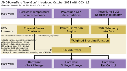
[[File:AMD PowerTune Bonaire.svg|thumb|Architecture of a newer version of PowerTune introduced with [[Graphics Core Next#1.1|GCN1.1]]-chips |
[[File:AMD PowerTune Bonaire.svg|thumb|Architecture of a newer version of PowerTune introduced with [[Graphics Core Next#1.1|GCN1.1]]-chips]] |
||
{{Main|AMD PowerTune}} |
{{Main|AMD PowerTune}} |
||
AMD PowerTune, [[dynamic frequency scaling]] for GPUs, was introduced with [[Radeon HD 6000 |
AMD PowerTune, [[dynamic frequency scaling]] for GPUs, was introduced with the [[Radeon HD 6000 series#Radeon HD 6900|Radeon HD 6900]] series on December 15, 2010 and has seen continued development, as documented in some reviews by [[AnandTech]].<ref>{{cite web |url=http://www.anandtech.com/show/4061/amds-radeon-hd-6970-radeon-hd-6950/7 |title=Redefining TDP With PowerTune |publisher=AnandTech |date=December 15, 2010 |access-date=April 30, 2015}}</ref><ref>{{cite web |url=http://www.anandtech.com/show/6025/radeon-hd-7970-ghz-edition-review-catching-up-to-gtx-680/2 |title=Introducing PowerTune Technology With Boost |publisher=AnandTech |date=June 22, 2012 |access-date=April 30, 2015}}</ref><ref>{{cite web |url=http://www.anandtech.com/show/6837/amd-radeon-7790-review-feat-sapphire-the-first-desktop-sea-islands/3 |title=The New PowerTune: Adding Further States |publisher=AnandTech |date=March 22, 2013 |access-date=April 30, 2015}}</ref><ref>{{cite web |url=http://www.anandtech.com/show/7457/the-radeon-r9-290x-review/5 |title=PowerTune: Improved Flexibility & Fan Speed Throttling |publisher=AnandTech |date=October 23, 2014 |access-date=April 30, 2015}}</ref> |
||
===Chips=== |
=== Chips === |
||
* Northern Islands chips: |
* Northern Islands chips: |
||
** Cayman RV970 |
** Cayman RV970 |
||
** Turks RV930 |
|||
** Barts RV940 |
|||
** Caïcos RV910 |
|||
** Antilles R900 |
** Antilles R900 |
||
** Trinity and Richland include a TeraScale 3 IGP |
** Trinity and Richland include a TeraScale 3 IGP |
||
==Successor== |
== Successor == |
||
{{Main|Graphics Core Next#first|l1= |
{{Main|Graphics Core Next#first|l1=Graphics Core Next 1.0}} |
||
At [[High-Performance Graphics|HPG11]] in August 2011 [[Advanced Micro Devices|AMD]] employees Michael Mantor (Senior Fellow Architect) and Mike Houston (Fellow Architect) presented [[Graphics Core Next]], the microarchitecture succeeding TeraScale.<ref>{{cite web |url=http://highperformancegraphics.org/previous/www_2011/media/Hot3D/HPG2011_Hot3D_AMD.pdf |title=AMD "Graphic Core Next": Low Power High Performance Graphics & Parallel Computer |date=2011 |
At [[High-Performance Graphics|HPG11]] in August 2011 [[Advanced Micro Devices|AMD]] employees Michael Mantor (Senior Fellow Architect) and Mike Houston (Fellow Architect) presented [[Graphics Core Next]], the microarchitecture succeeding TeraScale.<ref>{{cite web |url=http://highperformancegraphics.org/previous/www_2011/media/Hot3D/HPG2011_Hot3D_AMD.pdf |title=AMD "Graphic Core Next": Low Power High Performance Graphics & Parallel Computer |date=August 5, 2011 |access-date=July 6, 2014}}</ref> |
||
== Comparison of TeraScale chips == |
|||
{| class="wikitable" style="font-size: 85%; text-align: center;" |
|||
|- |
|||
! Microarchitecture |
|||
! colspan="12" | TeraScale 1 |
|||
! colspan="7" | TeraScale 2 |
|||
! TeraScale 3 |
|||
|- |
|||
! Chip<sup>1</sup> |
|||
! R600 |
|||
! RV610 |
|||
! RV620 |
|||
! RV630 |
|||
! RV635 |
|||
! RV670 |
|||
! RV710 |
|||
! RV711 |
|||
! RV730 |
|||
! RV740 |
|||
! RV770 |
|||
! RV790 |
|||
! Cedar<br />(RV810) |
|||
! Redwood<br />(RV830) |
|||
! Juniper<br />(RV840) |
|||
! Cypress<br />(RV870) |
|||
! Caicos<br />(RV910) |
|||
! Turks<br />(RV930) |
|||
! Barts<br />(RV940) |
|||
! Cayman<br />(RV970) |
|||
|- |
|||
! [[Code name]] |
|||
| ''Pele'' |
|||
| ''Laka'' |
|||
| ''Koopa'' |
|||
| ''Shaka'' |
|||
| ''Wario'' |
|||
| ''Boom'' |
|||
| colspan="2" | ''Luigi'' |
|||
| ''Mario'' |
|||
| ''Walden'' |
|||
| ''Wekiva'' |
|||
| ''Spartan'' |
|||
| ''?'' |
|||
| ''?'' |
|||
| ''?'' |
|||
| ''?'' |
|||
| ''?'' |
|||
| ''?'' |
|||
| ''Victoria'' |
|||
| ''?'' |
|||
|- |
|||
! Chip variant(s) |
|||
| {{N/a}} |
|||
| style="vertical-align:top;" | M72<br />M74 |
|||
| style="vertical-align:top;" | M82 |
|||
| style="vertical-align:top;" | M76 |
|||
| style="vertical-align:top;" | M86 |
|||
| style="vertical-align:top;" | M88 |
|||
| style="vertical-align:top;" | M92 |
|||
| style="vertical-align:top;" | M93 |
|||
| style="vertical-align:top;" | M96 |
|||
| style="vertical-align:top;" | M97 |
|||
| style="vertical-align:top;" | M98 |
|||
| {{N/a}} |
|||
| style="vertical-align:top;" | Park<br />Robson |
|||
| style="vertical-align:top;" | Capilano<br />Madison<br />Pinewood |
|||
| style="vertical-align:top;" | Broadway<br />Granville |
|||
| style="vertical-align:top;" | Hemlock<br />Lexington |
|||
| style="vertical-align:top;" | Seymour |
|||
| style="vertical-align:top;" | Onega<br />Thames<br />Whistler |
|||
| style="vertical-align:top;" | Blackcomb |
|||
| style="vertical-align:top;" | Antilles |
|||
|- |
|||
! [[Semiconductor device fabrication|Fab]] (nm) |
|||
| 80 |
|||
| 65 |
|||
| 55 |
|||
| 65 |
|||
| colspan="5" | 55 |
|||
| 40 |
|||
| colspan="2" | 55 |
|||
| colspan="8" | 40 |
|||
|- |
|||
! Die size (mm<sup>2</sup>) |
|||
| 420 || 85 / 82 (M74) || 67 || 153 || 135 || 192 || colspan="2" | 73 || 146 || 137 || 256 || 282 || 59 || 104 || 166 || 334 || 67 || 118 / 104 (Thames, Whistler) || 255 / 212 (Blackcomb) || 389 |
|||
|- |
|||
! Transistors (million) |
|||
| 720 || 180 || 181 || 390 || 378 || 666 || colspan="2" | 242 || 514 || 826 || 956 || 959 || 292 || 627 || 1,040 || 2,154 || 370 || 716 || 1,700 || 2,640 |
|||
|- |
|||
! Transistor density<br />(MTr/mm<sup>2</sup>) |
|||
| 1.7 || 2.1 / 2.2 (M74) || 2.7 || 2.5 || 2.8 || 3.5 || colspan="2" | 3.3 || 3.5 || 6.0 || 3.7 || 3.4 || 4.9 || 6.0 || 6.3 || 6.4 || 5.5 || 6.1 / 6.9 (Thames, Whistler) || 6.7 / 8.0 (Blackcomb) || 6.8 |
|||
|- |
|||
! Compute units |
|||
| 4 || colspan="2" | 2 || colspan="2" | 3 || 4 || colspan="2" | 1 || 4 || 8 || colspan="2" | 10 || 2 || 5 || 10 || 20 / 5 (Lexington) || 2 || 6 || 14 || 24 |
|||
|- |
|||
! Thread processors |
|||
| 16 || colspan="2" | 4 || colspan="2" | 8 || 16 || colspan="2" | 8 || colspan="2" | 32 || colspan="2" | 40 || 8 || 20 || 40 || 80 / 20 (Lexington) || 8 || 24 || 56 || 96 |
|||
|- |
|||
! [[Unified shader model|Stream processors]] |
|||
| 320 || colspan="2" | 40 || colspan="2" | 120 || 320 || colspan="2" | 80 || 320 || 640 || colspan="2" | 800 || 80 || 400 || 800 || 1600 / 400 (Lexington) || 160 || 480 || 1120 || 1536 |
|||
|- |
|||
! [[Texture mapping unit]]s |
|||
| 16 || colspan="2" | 4 || colspan="2" | 8 || 16 || colspan="2" | 8 || colspan="2" | 32 || colspan="2" | 40 || 8 || 20 || 40 || 80 / 20 (Lexington) || 8 || 24 || 56 || 96 |
|||
|- |
|||
! [[Render output unit]]s |
|||
| 16 || colspan="4" | 4 || 16 || colspan="2" | 4 || 8 || colspan="3" | 16 || 4 || 8 || 16 || 32 / 8 (Lexington) || 4 || 8 || 32 || 32 |
|||
|- |
|||
! [[Stencil buffer|{{abbr|Z/Stencil OPS|Z/Stencil render output units}}]] |
|||
| 32 || colspan="4" | 8 || 32 || colspan="2" | 4 || 32 || colspan="3" | 64 || 4 || colspan="3" | 40 || 16 || 32 || 40 || 128 |
|||
|- |
|||
! L1 [[Cache (computing)#Examples of hardware caches|cache]] (KB) |
|||
| colspan="6" | 32 per 4 SPs (Stream processors) || colspan="6" | 16 per CU (Compute unit) || colspan="8" | 8 per CU |
|||
|- |
|||
! L2 cache (KB) |
|||
| 256 || 32 || colspan="2" | 64 || 128 || 256 || colspan="2" | 64 || colspan="2" | 128 || colspan="2" | 256 || 128 || colspan="2" | 256 || 512 / 256 (Lexington) || 128 || 256 || colspan="2" | 512 |
|||
|- |
|||
! Display Core Engine |
|||
| colspan="2" | 2.0 || 3.0 || 2.0 || 3.0 || 2.0 || colspan="4" | 3.2 || colspan="2" | 3.1 || colspan="4" | 4.0 || colspan="4" | 5.0 |
|||
|- |
|||
! [[Unified Video Decoder]] |
|||
| [[ATI Avivo|Avivo HD]] || colspan="5" | 1.0 || colspan="4" | 2.2 || colspan="2" | 2.0 || colspan="4" | 2.3 || colspan="4" | 3.1 |
|||
|- |
|||
! Initial launch |
|||
| {{dts|2007|May||format=my|abbr=on}} |
|||
| {{dts|2007|January||format=my|abbr=on}} |
|||
| {{dts|2008|January||format=my|abbr=on}} |
|||
| {{dts|2007|June||format=my|abbr=on}} |
|||
| {{dts|2008|January||format=my|abbr=on}} |
|||
| {{dts|2007|November||format=my|abbr=on}} |
|||
| {{dts|2008|September||format=my|abbr=on}} |
|||
| {{dts|2010|May||format=my|abbr=on}} |
|||
| {{dts|2008|September||format=my|abbr=on}} |
|||
| {{dts|2009|April||format=my|abbr=on}} |
|||
| {{dts|2008|June||format=my|abbr=on}} |
|||
| {{dts|2009|April||format=my|abbr=on}} |
|||
| {{dts|2010|February||format=my|abbr=on}} |
|||
| {{dts|2010|January||format=my|abbr=on}} |
|||
| {{dts|2009|October||format=my|abbr=on}} |
|||
| {{dts|2009|September||format=my|abbr=on}} |
|||
| colspan="2" | {{dts|2011|February||format=my|abbr=on}} |
|||
| {{dts|2010|October||format=my|abbr=on}} |
|||
| {{dts|2010|December||format=my|abbr=on}} |
|||
|- |
|||
! Series |
|||
| colspan="6" | R600 ([[Radeon HD 2000 series|Radeon HD 2000]] / [[Radeon HD 3000 series|Radeon HD 3000]]) |
|||
| colspan="6" | R700 ([[Radeon HD 4000 series|Radeon HD 4000]]) |
|||
| colspan="4" | Evergreen ([[Radeon HD 5000 series|Radeon HD 5000]]) |
|||
| colspan="4" | Northern Islands ([[Radeon HD 6000 series|Radeon HD 6000]]) |
|||
|- |
|||
! References |
|||
| <ref name="R600-techpowerup">{{Cite web |title=ATI R600 GPU Specs |url=https://www.techpowerup.com/gpu-specs/ati-r600.g431 |access-date=December 21, 2022 |website=TechPowerUp}}</ref><ref name="R600-videocardz">{{Cite web |title=ATI R600 GPU |url=https://videocardz.net/gpu/ati-r600 |access-date=December 21, 2022 |website=VideoCardz}}</ref> |
|||
| <ref name="RV610-techpowerup">{{Cite web |title=ATI RV610 GPU Specs |url=https://www.techpowerup.com/gpu-specs/ati-rv610.g55 |access-date=December 21, 2022 |website=TechPowerUp}}</ref><ref name="RV610-videocardz">{{Cite web |title=ATI RV610 GPU |url=https://videocardz.net/gpu/ati-rv610 |access-date=December 21, 2022 |website=VideoCardz}}</ref><br /><ref name="M72-techpowerup">{{Cite web |title=ATI M72 GPU Specs |url=https://www.techpowerup.com/gpu-specs/ati-m72.g260 |access-date=December 21, 2022 |website=TechPowerUp}}</ref><ref name="M74-techpowerup">{{Cite web |title=ATI M74 GPU Specs |url=https://www.techpowerup.com/gpu-specs/ati-m74.g660 |access-date=December 21, 2022 |website=TechPowerUp}}</ref> |
|||
| <ref name="RV620-techpowerup">{{Cite web |title=ATI RV620 GPU Specs |url=https://www.techpowerup.com/gpu-specs/ati-rv620.g63 |access-date=December 21, 2022 |website=TechPowerUp}}</ref><ref name="RV620-videocardz">{{Cite web |title=ATI RV620 GPU |url=https://videocardz.net/gpu/ati-rv620 |access-date=December 21, 2022 |website=VideoCardz}}</ref><br /><ref name="M82-techpowerup">{{Cite web |title=ATI M82 GPU Specs |url=https://www.techpowerup.com/gpu-specs/ati-m82.g195 |access-date=December 21, 2022 |website=TechPowerUp}}</ref> |
|||
| <ref name="RV630-techpowerup">{{Cite web |title=ATI RV630 GPU Specs |url=https://www.techpowerup.com/gpu-specs/ati-rv630.g54 |access-date=December 21, 2022 |website=TechPowerUp}}</ref><ref name="RV630-videocardz">{{Cite web |title=ATI RV630 GPU |url=https://videocardz.net/gpu/ati-rv630 |access-date=December 21, 2022 |website=VideoCardz}}</ref><br /><ref name="M76-techpowerup">{{Cite web |title=ATI M76 GPU Specs |url=https://www.techpowerup.com/gpu-specs/ati-m76.g262 |access-date=December 21, 2022 |website=TechPowerUp}}</ref> |
|||
| <ref name="RV635-techpowerup">{{Cite web |title=ATI RV635 GPU Specs |url=https://www.techpowerup.com/gpu-specs/ati-rv635.g65 |access-date=December 21, 2022 |website=TechPowerUp}}</ref><ref name="RV635-videocardz">{{Cite web |title=ATI RV635 GPU |url=https://videocardz.net/gpu/ati-rv635 |access-date=December 21, 2022 |website=VideoCardz}}</ref><br /><ref name="M86-techpowerup">{{Cite web |title=ATI M86 GPU Specs |url=https://www.techpowerup.com/gpu-specs/ati-m86.g234 |access-date=December 21, 2022 |website=TechPowerUp}}</ref> |
|||
| <ref name="RV670-techpowerup">{{Cite web |title=ATI RV670 GPU Specs |url=https://www.techpowerup.com/gpu-specs/ati-rv670.g59 |access-date=December 21, 2022 |website=TechPowerUp}}</ref><ref name="RV670-videocardz">{{Cite web |title=ATI RV670 GPU |url=https://videocardz.net/gpu/ati-rv670 |access-date=December 21, 2022 |website=VideoCardz}}</ref><br /><ref name="M88-techpowerup">{{Cite web |title=ATI M88 GPU Specs |url=https://www.techpowerup.com/gpu-specs/ati-m88.g270 |access-date=December 21, 2022 |website=TechPowerUp}}</ref> |
|||
| <ref name="RV710-techpowerup">{{Cite web |title=ATI RV710 GPU Specs |url=https://www.techpowerup.com/gpu-specs/ati-rv710.g69 |access-date=December 21, 2022 |website=TechPowerUp}}</ref><ref name="RV710-videocardz">{{Cite web |title=ATI RV710 GPU |url=https://videocardz.net/gpu/ati-rv710 |access-date=December 21, 2022 |website=VideoCardz}}</ref><br /><ref name="M92-techpowerup">{{Cite web |title=ATI M92 GPU Specs |url=https://www.techpowerup.com/gpu-specs/ati-m92.g273 |access-date=December 21, 2022 |website=TechPowerUp}}</ref> |
|||
| <ref name="RG220-gpuzoo">{{Cite web |title=ATI FirePro RG220 GPU specs |url=https://www.gpuzoo.com/GPU-ATI/FirePro_RG220.html |access-date=December 21, 2022 |website=GPUZoo}}</ref><br /><ref name="M93-techpowerup">{{Cite web |title=ATI M93 GPU Specs |url=https://www.techpowerup.com/gpu-specs/ati-m93.g139 |access-date=December 21, 2022 |website=TechPowerUp}}</ref> |
|||
| <ref name="RV730-techpowerup">{{Cite web |title=ATI RV730 GPU Specs |url=https://www.techpowerup.com/gpu-specs/ati-rv730.g70 |access-date=December 21, 2022 |website=TechPowerUp}}</ref><ref name="RV730-videocardz">{{Cite web |title=ATI RV730 GPU |url=https://videocardz.net/gpu/ati-rv730 |access-date=December 21, 2022 |website=VideoCardz}}</ref><br /><ref name="M96-techpowerup">{{Cite web |title=ATI M96 GPU Specs |url=https://www.techpowerup.com/gpu-specs/ati-m96.g124 |access-date=December 21, 2022 |website=TechPowerUp}}</ref> |
|||
| <ref name="RV740-techpowerup">{{Cite web |title=ATI RV740 GPU Specs |url=https://www.techpowerup.com/gpu-specs/ati-rv740.g95 |access-date=December 21, 2022 |website=TechPowerUp}}</ref><ref name="RV740-videocardz">{{Cite web |title=ATI RV740 GPU |url=https://videocardz.net/gpu/ati-rv740 |access-date=December 21, 2022 |website=VideoCardz}}</ref><br /><ref name="M97-techpowerup">{{Cite web |title=ATI M97 GPU Specs |url=https://www.techpowerup.com/gpu-specs/ati-m97.g276 |access-date=December 21, 2022 |website=TechPowerUp}}</ref> |
|||
| <ref name="RV770-techpowerup">{{Cite web |title=ATI RV770 GPU Specs |url=https://www.techpowerup.com/gpu-specs/ati-rv770.g62 |access-date=December 21, 2022 |website=TechPowerUp}}</ref><ref name="RV770-videocardz">{{Cite web |title=ATI RV770 GPU |url=https://videocardz.net/gpu/ati-rv770 |access-date=December 21, 2022 |website=VideoCardz}}</ref><br /><ref name="M98-techpowerup">{{Cite web |title=ATI M98 GPU Specs |url=https://www.techpowerup.com/gpu-specs/ati-m98.g277 |access-date=December 21, 2022 |website=TechPowerUp}}</ref> |
|||
| <ref name="RV790-techpowerup">{{Cite web |title=ATI RV790 GPU Specs |url=https://www.techpowerup.com/gpu-specs/ati-rv790.g432 |access-date=December 21, 2022 |website=TechPowerUp}}</ref><ref name="RV790-videocardz">{{Cite web |title=ATI RV790 GPU |url=https://videocardz.net/gpu/ati-rv790 |access-date=December 21, 2022 |website=VideoCardz}}</ref> |
|||
| <ref name="cedar-techpowerup">{{Cite web |title=ATI Cedar GPU Specs |url=https://www.techpowerup.com/gpu-specs/ati-cedar.g79 |access-date=December 22, 2022 |website=TechPowerUp}}</ref><ref name="cedar-videocardz">{{Cite web |title=ATI Cedar GPU |url=https://videocardz.net/gpu/ati-cedar |access-date=December 22, 2022 |website=VideoCardz}}</ref><br /><ref name="park-techpowerup">{{Cite web |title=ATI Park GPU Specs |url=https://www.techpowerup.com/gpu-specs/ati-park.g279 |access-date=December 22, 2022 |website=TechPowerUp}}</ref><ref name="robson-techpowerup">{{Cite web |title=AMD Robson GPU Specs |url=https://www.techpowerup.com/gpu-specs/amd-robson.g106 |access-date=December 22, 2022 |website=TechPowerUp}}</ref> |
|||
| <ref name="redwood-techpowerup">{{Cite web |title=ATI Redwood GPU Specs |url=https://www.techpowerup.com/gpu-specs/ati-redwood.g75 |access-date=December 22, 2022 |website=TechPowerUp}}</ref><ref name="redwood-videocardz">{{Cite web |title=ATI Redwood GPU |url=https://videocardz.net/gpu/ati-redwood |access-date=December 22, 2022 |website=VideoCardz}}</ref><br /><ref name="capilano-techpowerup">{{Cite web |title=AMD Capilano GPU Specs |url=https://www.techpowerup.com/gpu-specs/amd-capilano.g104 |access-date=December 22, 2022 |website=TechPowerUp}}</ref><ref name="madison-techpowerup">{{Cite web |title=ATI Madison GPU Specs |url=https://www.techpowerup.com/gpu-specs/ati-madison.g282 |access-date=December 22, 2022 |website=TechPowerUp}}</ref><ref name="pinewood-techpowerup">{{Cite web |title=ATI Pinewood GPU Specs |url=https://www.techpowerup.com/gpu-specs/ati-pinewood.g863 |access-date=December 22, 2022 |website=TechPowerUp}}</ref> |
|||
| <ref name="juniper-techpowerup">{{Cite web |title=ATI Juniper GPU Specs |url=https://www.techpowerup.com/gpu-specs/ati-juniper.g122 |access-date=December 22, 2022 |website=TechPowerUp}}</ref><br /><ref name="broadway-techpowerup">{{Cite web |title=AMD Broadway GPU Specs |url=https://www.techpowerup.com/gpu-specs/ati-broadway.g107 |access-date=December 22, 2022 |website=TechPowerUp}}</ref><ref name="granville-techpowerup">{{Cite web |title=AMD Granville GPU Specs |url=https://www.techpowerup.com/gpu-specs/amd-granville.g102 |access-date=December 22, 2022 |website=TechPowerUp}}</ref> |
|||
| <ref name="cypress-techpowerup">{{Cite web |title=ATI Cypress GPU Specs |url=https://www.techpowerup.com/gpu-specs/ati-cypress.g77 |access-date=December 22, 2022 |website=TechPowerUp}}</ref><ref name="cypress-videocardz">{{Cite web |title=ATI Cypress GPU |url=https://videocardz.net/gpu/ati-cypress |access-date=December 22, 2022 |website=VideoCardz}}</ref><br /><ref name="hemlock-techpowerup">{{Cite web |title=ATI Hemlock GPU Specs |url=https://www.techpowerup.com/gpu-specs/ati-hemlock.g78 |access-date=December 22, 2022 |website=TechPowerUp}}</ref><ref name="lexington-techpowerup">{{Cite web |title=AMD Lexington GPU Specs |url=https://www.techpowerup.com/gpu-specs/amd-lexington.g867 |access-date=December 22, 2022 |website=TechPowerUp}}</ref> |
|||
| <ref name="caicos-techpowerup">{{Cite web |title=AMD Caicos GPU Specs |url=https://www.techpowerup.com/gpu-specs/amd-caicos.g114 |access-date=December 22, 2022 |website=TechPowerUp}}</ref><ref name="caicos-videocardz">{{Cite web |title=AMD Caicos GPU |url=https://videocardz.net/gpu/amd-caicos |access-date=December 22, 2022 |website=VideoCardz}}</ref><br /><ref name="seymour-techpowerup">{{Cite web |title=AMD Seymour GPU Specs |url=https://www.techpowerup.com/gpu-specs/amd-seymour.g105 |access-date=December 22, 2022 |website=TechPowerUp}}</ref> |
|||
| <ref name="turks-techpowerup">{{Cite web |title=AMD Turks GPU Specs |url=https://www.techpowerup.com/gpu-specs/amd-turks.g92 |access-date=December 22, 2022 |website=TechPowerUp}}</ref><ref name="turks-videocardz">{{Cite web |title=ATI Turks GPU |url=https://videocardz.net/gpu/ati-turks |access-date=December 22, 2022 |website=VideoCardz}}</ref><br /><ref name="onega-techpowerup">{{Cite web |title=AMD Onega GPU Specs |url=https://www.techpowerup.com/gpu-specs/amd-onega.g377 |access-date=December 22, 2022 |website=TechPowerUp}}</ref><ref name="thames-techpowerup">{{Cite web |title=AMD Thames GPU Specs |url=https://www.techpowerup.com/gpu-specs/amd-thames.g197 |access-date=December 22, 2022 |website=TechPowerUp}}</ref><ref name="whistler-techpowerup">{{Cite web |title=AMD Whistler GPU Specs |url=https://www.techpowerup.com/gpu-specs/amd-whistler.g103 |access-date=December 22, 2022 |website=TechPowerUp}}</ref> |
|||
| <ref name="barts-techpowerup">{{Cite web |title=AMD Barts GPU Specs |url=https://www.techpowerup.com/gpu-specs/amd-barts.g80 |access-date=December 22, 2022 |website=TechPowerUp}}</ref><ref name="barts-videocardz">{{Cite web |title=AMD Barts GPU |url=https://videocardz.net/gpu/amd-barts |access-date=December 22, 2022 |website=VideoCardz}}</ref><br /><ref name="blackcomb-techpowerup">{{Cite web |title=AMD Blackcomb GPU Specs |url=https://www.techpowerup.com/gpu-specs/amd-blackcomb.g101 |access-date=December 22, 2022 |website=TechPowerUp}}</ref> |
|||
| <ref name="cayman-techpowerup">{{Cite web |title=AMD Cayman GPU Specs |url=https://www.techpowerup.com/gpu-specs/amd-cayman.g81 |access-date=December 22, 2022 |website=TechPowerUp}}</ref><ref name="cayman-videocardz">{{Cite web |title=AMD Cayman GPU |url=https://videocardz.net/gpu/amd-cayman |access-date=December 22, 2022 |website=VideoCardz}}</ref><br /><ref name="antilles-techpowerup">{{Cite web |title=AMD Antilles GPU Specs |url=https://www.techpowerup.com/gpu-specs/amd-antilles.g90 |access-date=December 22, 2022 |website=TechPowerUp}}</ref> |
|||
|} |
|||
<sup>1</sup> Duo chips such as R680 (2x RV670) and R700 (2x RV770) are not listed.<ref name="R680-techpowerup">{{Cite web |title=ATI R680 GPU Specs |url=https://www.techpowerup.com/gpu-specs/ati-r680.g121 |access-date=December 21, 2022 |website=TechPowerUp}}</ref><ref name="HD3870x2-videocardz">{{Cite web |title=ATI Radeon HD 3870 X2 |url=https://videocardz.net/ati-radeon-hd-3870-x2 |access-date=December 21, 2022 |website=VideoCardz}}</ref><ref name="R700-techpowerup">{{Cite web |title=ATI R700 GPU Specs |url=https://www.techpowerup.com/gpu-specs/ati-r700.g645 |access-date=December 21, 2022 |website=TechPowerUp}}</ref><ref name="HD4870x2-videocardz">{{Cite web |title=ATI Radeon HD 4870 X2 |url=https://videocardz.net/ati-radeon-hd-4870-x2 |access-date=December 21, 2022 |website=VideoCardz}}</ref> |
|||
==References== |
== References == |
||
{{reflist|30em}} |
{{reflist|30em}} |
||
{{AMD graphics}} |
{{AMD graphics}} |
||
[[Category: |
[[Category:AMD microarchitectures]] |
||
[[Category:GPGPU]] |
[[Category:GPGPU]] |
||
[[Category:Graphics microarchitectures|Radeon TeraScale]] |
[[Category:Graphics microarchitectures|Radeon TeraScale]] |
||
Latest revision as of 09:33, 4 April 2024
This article needs additional citations for verification. (March 2021) |
TeraScale is the codename for a family of graphics processing unit microarchitectures developed by ATI Technologies/AMD and their second microarchitecture implementing the unified shader model following Xenos. TeraScale replaced the old fixed-pipeline microarchitectures and competed directly with Nvidia's first unified shader microarchitecture named Tesla.[1][2]
TeraScale was used in Radeon HD 2000 manufactured in 80 nm and 65 nm, Radeon HD 3000 manufactured in 65 nm and 55 nm, Radeon HD 4000 manufactured in 55 nm and 40 nm, Radeon HD 5000 and Radeon HD 6000 manufactured in 40 nm. TeraScale was also used in the AMD Accelerated Processing Units code-named "Brazos", "Llano", "Trinity" and "Richland". TeraScale is even found in some of the succeeding graphics cards brands.
TeraScale is a VLIW SIMD architecture, while Tesla is a RISC SIMD architecture, similar to TeraScale's successor Graphics Core Next. TeraScale implements HyperZ.[3]
An LLVM code generator (i.e. a compiler back-end) is available for TeraScale,[4] but it seems to be missing in LLVM's matrix.[5] E.g. Mesa 3D makes use of it.
TeraScale 1 (VLIW)[edit]
| Release date | May 2007[citation needed] |
|---|---|
| History | |
| Predecessor | Not publicly known[citation needed] |
| Successor | TeraScale 2 |
| Support status | |
| Unsupported | |
At SIGGRAPH 08 in December 2008, AMD employee Mike Houston described some of the TeraScale microarchitecture.[6]
At FOSDEM09 Matthias Hopf from AMDs technology partner SUSE Linux presented a slide regarding the programming of open-source driver for the R600.[7]
Unified shaders[edit]
Previous GPU architectures implemented fixed-pipelines, i.e. there were distinct shader processors for each type of shader. TeraScale leverages many flexible shader processors which can be scheduled to process a variety of shader types, thereby significantly increasing GPU throughput (dependent on application instruction mix as noted below). The R600 core processes vertex, geometry, and pixel shaders as outlined by the Direct3D 10.0 specification for Shader Model 4.0 in addition to full OpenGL 3.0 support.[8]
The new unified shader functionality is based upon a very long instruction word (VLIW) architecture in which the core executes operations in parallel.[9]
A shader cluster is organized into 5 stream processing units. Each stream processing unit can retire a finished single precision floating point MAD (or ADD or MUL) instruction per clock, dot product (DP, and special cased by combining ALUs), and integer ADD.[10] The 5th unit is more complex and can additionally handle special transcendental functions such as sine and cosine.[10] Each shader cluster can execute 6 instructions per clock cycle (peak), consisting of 5 shading instructions plus 1 branch.[10]
Notably, the VLIW architecture brings with it some classic challenges inherent to VLIW designs, namely that of maintaining optimal instruction flow.[9] Additionally, the chip cannot co-issue instructions when one is dependent on the results of the other. Performance of the GPU is highly dependent on the mixture of instructions being used by the application and how well the real-time compiler in the driver can organize said instructions.[10]
R600 core includes 64 shader clusters, while RV610 and RV630 cores have 8 and 24 shader clusters respectively.
Hardware tessellation[edit]
TeraScale includes multiple units capable of carrying out tessellation. Those are similar to the programmable units of the Xenos GPU which is used in the Xbox 360.
Tessellation was officially specified in the major API's starting with DirectX 11 and OpenGL 4. TeraScale 1 based GPU's (HD 2000, 3000 and 4000 series) are only conformant to Direct3D 10 and OpenGL 3.3 and implements therefore a different tessellation principle which uses vendor specific API extensions.[11] The TeraScale 2 based GPU's (starting with the Radeon HD 5000 series) were the first to conform with both Direct3D 11 and OpenGL 4.0 tesselation technique.[12] Although the TeraScale 1 tessellator is simpler in design, it is described by AMD as a subset of the later tesselation standard.[13]
The TeraScale tessellator units allow the developers to take a simple polygon mesh and subdivide it using a curved surface evaluation function. There are different tessellation forms, such as Bézier surfaces with N-patches, B-splines and NURBS, and also some subdivision techniques of the surface, which usually includes displacement map some kind of a texture.[14] Essentially, this allows a simple, low-polygon model to be increased dramatically in polygon density in real-time with very small impact on the performance. Scott Wasson of Tech Report noted during an AMD demo that the resulting model was so dense with millions of polygons that it appeared to be solid.[9]
The TeraScale tessellator is reminiscent of ATI TruForm, the brand name of an early hardware tessellation unit used initially in the Radeon 8500.[15]
ATI TruForm received little attention from software developers. A few games (such as Madden NFL 2004, Serious Sam, Unreal Tournament 2003 and 2004, and unofficially Morrowind), had the support for the ATI's tesselation technology included. Such a slow adaptation has to do with the fact that it was not a feature shared with NVIDIA GPUs, since those had implemented a competing tessellation solution using Quintic-RT patches which had achieved even less support from the major game developers.[16] Since the Xbox 360's GPU is based on the ATI's architecture, Microsoft saw the hardware-accelerated surface tessellation as a major GPU feature. A couple of years later the tesselation feature became mandatory with the release of the DirectX 11 in 2009.[14][17]
While the tessellation principle introduced with TeraScale was not part of the OpenGL 3.3 or Direct3D 10.0 requirements, and competitors such as the GeForce 8 series lacked similar hardware, Microsoft has added the tessellation feature as part of their DirectX 10.1 future plans.[17] Finally, Microsoft introduced tessellation as a required capability not with DirectX 10.1 but DirectX 11.[18]
GCN geometric processor is AMD's (which acquired the ATI's GPU business) most current solution for carrying out tessellation using the GPU.
Ultra-threaded dispatch processor[edit]
Although the R600 is a significant departure from previous designs, it still shares many features with its predecessor, the Radeon R520.[9] The Ultra-Threaded Dispatch Processor is a major architectural component of the R600 core, just as it was with the Radeon X1000 GPUs. This processor manages a large number of in-flight threads of three distinct types (vertex, geometry, and pixel shaders) and switches amongst them as needed.[9] With a large number of threads being managed simultaneously it is possible to reorganize thread order to optimally utilize the shaders. In other words, the dispatch processor evaluates what goes in the other parts of the R600 and attempts to keep processing efficiency as high as possible. There are lower levels of management as well; each SIMD array of 80 stream processors has its own sequencer and arbiter. The arbiter decides which thread to process next, while the sequencer attempts to reorder instructions for best possible performance within each thread.[9]
Texturing and anti-aliasing[edit]
Texturing and final output aboard the R600 core is similar but also distinct from R580. R600 is equipped with 4 texture units that are decoupled (independent) from the shader core, like in the R520 and R580 GPUs.[9] The render output units (ROPs) of Radeon HD 2000 series now performs the task of Multisample anti-aliasing (MSAA) with programmable sample grids and maximum of 8 sample points, instead of using pixel shaders as in the Radeon X1000 series. Also new is the capability to filter FP16 textures, popular with HDR lighting, at full-speed. ROP can also perform trilinear and anisotropic filtering on all texture formats. On R600, this totals 16 pixels per clock for FP16 textures, while higher precision FP32 textures filter at half-speed (8 pixels per clock).[9]
Anti-aliasing capabilities are more robust on R600 than on the R520 series. In addition to the ability to perform 8× MSAA, up from 6× MSAA on the R300 through R580, R600 has a new custom filter anti-aliasing (CFAA) mode. CFAA refers to an implementation of non-box filters that look at pixels around the particular pixel being processed in order to calculate the final color and anti-alias the image.[10] CFAA is performed by shader, instead of in the ROPs. This brings greatly enhanced programmability because the filters can be customized, but may also bring potential performance issues because of the use of shader resources. As of launch of R600, CFAA utilizes wide and narrow tent filters. With these, samples from outside the pixel being processed are weighted linearly based upon their distance from the centroid of that pixel, with the linear function adjusted based on the wide or narrow filter chosen.[10]
Memory controllers[edit]
Memory controllers are connected via internal bi-directional ring bus wrapped around the processor. In Radeon HD 2900, it is a 1,024-bit bi-directional ring bus (512-bit read and 512-bit write), with 8 64-bit memory channels for a total bus width of 512-bits on the 2900 XT.;[9] in Radeon HD 3800, it is a 512-bit ring bus; in Radeon HD 2600 and HD 3600, it is a 256-bit ring bus; In Radeon HD 2400 and HD 3400, there is no ring bus.
Half-generation update[edit]
This section needs expansion. You can help by adding to it. (May 2009) |
The series saw a half-generation update with die shrink (55 nm) variants: RV670, RV635 and RV620. All variants support PCI Express 2.0, DirectX 10.1 with Shader Model 4.1 features, dedicated ATI Unified Video Decoder (UVD) for all models[19] and PowerPlay technology for desktop video cards.[20]
Except the Radeon HD 3800 series, all variants supported 2 integrated DisplayPort outputs, supporting 24- and 30-bit displays for resolutions up to 2,560×1,600. Each output included 1, 2, or 4 lanes per output, with data rate up to 2.7 Gbit/s per lane.
ATI claimed that the support of DirectX 10.1 can bring improved performance and processing efficiency with reduced rounding error (0.5 ULP compared with average error 1.0 ULP as tolerable error), better image details and quality, global illumination (a technique used in animated films, and more improvements to consumer gaming systems therefore giving more realistic gaming experience.[21] )
Video cards[edit]
(see list of chips in those pages)
TeraScale 2 (VLIW5)[edit]
| Release date | September 2009[citation needed] |
|---|---|
| History | |
| Predecessor | TeraScale 1 |
| Successor | TeraScale 3 |
| Support status | |
| Unsupported | |
TeraScale 2 (VLIW5) was introduced with Radeon HD 5000 series GPUs in "Evergreen" generation.
At HPG10 Mark Fowler presented the "Evergreen" and stated that e.g. 5870 (Cypress), 5770 (Juniper) and 5670 (Redwood) support max resolution of the 6 times 2560×1600 pixels, while the 5470 (Cedar) supports 4 times 2560×1600 pixels, important for AMD Eyefinity multi-monitor support.[22]
With the release of Cypress, the Terascale graphics engine architecture has been upgraded with twice the number of stream cores, texture units and ROP units compared to the RV770. The architecture of stream cores is largely unchanged, but adds support for DirectX 11/DirectCompute 11 capabilities with new instructions.[23] Also similar to RV770, four texture units are tied to 16 stream cores (each have five processing elements, making a total of 80 processing elements). This combination of is referred to as a SIMD core.
Unlike the predecessor Radeon R700, as DirectX 11 mandates full developer control over interpolation, dedicated interpolators were removed, relying instead on the SIMD cores. The stream cores can handle the higher rounding precision fused multiply–add (FMA) instruction in both single and double precision which increases precision over multiply–add (MAD) and is compliant to IEEE 754-2008 standard.[24] The instruction sum of absolute differences (SAD) has been natively added to the processors. This instruction can be used to greatly improve the performance of some processes, such as video encoding and transcoding on the 3D engine. Each SIMD core is equipped with 32 KiB local data share and 8 kiB of L1 cache,[23] while all SIMD cores share 64 KiB global data share.
Memory controller[edit]
Each memory controller ties to two quad ROPs, one per 64-bit channel, and dedicated 512 KiB L2 cache.[23]
Power saving[edit]
AMD PowerPlay is supported, see there.
Chips[edit]
- Evergreen chips:
- Cedar RV810
- Cypress RV870
- Hemlock R800
- Juniper RV840
- Redwood RV830
- Northern Islands chips:
- Barts RV940
- Caicos RV910
- Turks RV930
- APU that include a TeraScale 2 IGP:
- Llano
- Ontario
- Zacate
TeraScale 3 (VLIW4)[edit]
| Release date | October 2010[citation needed] |
|---|---|
| History | |
| Predecessor | TeraScale 2 |
| Successor | Graphics Core Next 1 |
| Support status | |
| Unsupported | |
TeraScale 3 (VLIW4) replaces the previous 5-way VLIW designs with a 4-way VLIW design. The new design also incorporates an additional tessellation unit to improve Direct3D 11 performance.
TeraScale 3 is introduced in the Radeon HD 6900-branded graphics cards and also implemented in the Trinity and Richland APUs.
Power saving[edit]
AMD PowerTune, dynamic frequency scaling for GPUs, was introduced with the Radeon HD 6900 series on December 15, 2010 and has seen continued development, as documented in some reviews by AnandTech.[25][26][27][28]
Chips[edit]
- Northern Islands chips:
- Cayman RV970
- Antilles R900
- Trinity and Richland include a TeraScale 3 IGP
Successor[edit]
At HPG11 in August 2011 AMD employees Michael Mantor (Senior Fellow Architect) and Mike Houston (Fellow Architect) presented Graphics Core Next, the microarchitecture succeeding TeraScale.[29]
Comparison of TeraScale chips[edit]
| Microarchitecture | TeraScale 1 | TeraScale 2 | TeraScale 3 | |||||||||||||||||
|---|---|---|---|---|---|---|---|---|---|---|---|---|---|---|---|---|---|---|---|---|
| Chip1 | R600 | RV610 | RV620 | RV630 | RV635 | RV670 | RV710 | RV711 | RV730 | RV740 | RV770 | RV790 | Cedar (RV810) |
Redwood (RV830) |
Juniper (RV840) |
Cypress (RV870) |
Caicos (RV910) |
Turks (RV930) |
Barts (RV940) |
Cayman (RV970) |
| Code name | Pele | Laka | Koopa | Shaka | Wario | Boom | Luigi | Mario | Walden | Wekiva | Spartan | ? | ? | ? | ? | ? | ? | Victoria | ? | |
| Chip variant(s) | — | M72 M74 |
M82 | M76 | M86 | M88 | M92 | M93 | M96 | M97 | M98 | — | Park Robson |
Capilano Madison Pinewood |
Broadway Granville |
Hemlock Lexington |
Seymour | Onega Thames Whistler |
Blackcomb | Antilles |
| Fab (nm) | 80 | 65 | 55 | 65 | 55 | 40 | 55 | 40 | ||||||||||||
| Die size (mm2) | 420 | 85 / 82 (M74) | 67 | 153 | 135 | 192 | 73 | 146 | 137 | 256 | 282 | 59 | 104 | 166 | 334 | 67 | 118 / 104 (Thames, Whistler) | 255 / 212 (Blackcomb) | 389 | |
| Transistors (million) | 720 | 180 | 181 | 390 | 378 | 666 | 242 | 514 | 826 | 956 | 959 | 292 | 627 | 1,040 | 2,154 | 370 | 716 | 1,700 | 2,640 | |
| Transistor density (MTr/mm2) |
1.7 | 2.1 / 2.2 (M74) | 2.7 | 2.5 | 2.8 | 3.5 | 3.3 | 3.5 | 6.0 | 3.7 | 3.4 | 4.9 | 6.0 | 6.3 | 6.4 | 5.5 | 6.1 / 6.9 (Thames, Whistler) | 6.7 / 8.0 (Blackcomb) | 6.8 | |
| Compute units | 4 | 2 | 3 | 4 | 1 | 4 | 8 | 10 | 2 | 5 | 10 | 20 / 5 (Lexington) | 2 | 6 | 14 | 24 | ||||
| Thread processors | 16 | 4 | 8 | 16 | 8 | 32 | 40 | 8 | 20 | 40 | 80 / 20 (Lexington) | 8 | 24 | 56 | 96 | |||||
| Stream processors | 320 | 40 | 120 | 320 | 80 | 320 | 640 | 800 | 80 | 400 | 800 | 1600 / 400 (Lexington) | 160 | 480 | 1120 | 1536 | ||||
| Texture mapping units | 16 | 4 | 8 | 16 | 8 | 32 | 40 | 8 | 20 | 40 | 80 / 20 (Lexington) | 8 | 24 | 56 | 96 | |||||
| Render output units | 16 | 4 | 16 | 4 | 8 | 16 | 4 | 8 | 16 | 32 / 8 (Lexington) | 4 | 8 | 32 | 32 | ||||||
| Z/Stencil OPS | 32 | 8 | 32 | 4 | 32 | 64 | 4 | 40 | 16 | 32 | 40 | 128 | ||||||||
| L1 cache (KB) | 32 per 4 SPs (Stream processors) | 16 per CU (Compute unit) | 8 per CU | |||||||||||||||||
| L2 cache (KB) | 256 | 32 | 64 | 128 | 256 | 64 | 128 | 256 | 128 | 256 | 512 / 256 (Lexington) | 128 | 256 | 512 | ||||||
| Display Core Engine | 2.0 | 3.0 | 2.0 | 3.0 | 2.0 | 3.2 | 3.1 | 4.0 | 5.0 | |||||||||||
| Unified Video Decoder | Avivo HD | 1.0 | 2.2 | 2.0 | 2.3 | 3.1 | ||||||||||||||
| Initial launch | May 2007 | Jan 2007 | Jan 2008 | Jun 2007 | Jan 2008 | Nov 2007 | Sep 2008 | May 2010 | Sep 2008 | Apr 2009 | Jun 2008 | Apr 2009 | Feb 2010 | Jan 2010 | Oct 2009 | Sep 2009 | Feb 2011 | Oct 2010 | Dec 2010 | |
| Series | R600 (Radeon HD 2000 / Radeon HD 3000) | R700 (Radeon HD 4000) | Evergreen (Radeon HD 5000) | Northern Islands (Radeon HD 6000) | ||||||||||||||||
| References | [30][31] | [32][33] [34][35] |
[36][37] [38] |
[39][40] [41] |
[42][43] [44] |
[45][46] [47] |
[48][49] [50] |
[51] [52] |
[53][54] [55] |
[56][57] [58] |
[59][60] [61] |
[62][63] | [64][65] [66][67] |
[68][69] [70][71][72] |
[73] [74][75] |
[76][77] [78][79] |
[80][81] [82] |
[83][84] [85][86][87] |
[88][89] [90] |
[91][92] [93] |
1 Duo chips such as R680 (2x RV670) and R700 (2x RV770) are not listed.[94][95][96][97]
References[edit]
- ^ Kevin Parrish (March 9, 2011). "The TeraScale 3 architecture of the HD 6990". Tom's Hardware. Retrieved April 8, 2015.
- ^ "Anatomy of AMD's TeraScale Graphics Engine" (PDF). Archived from the original (PDF) on June 13, 2010. Retrieved November 21, 2021.
- ^ "Feature matrix of the free and open-source "Radeon" graphics device driver". Retrieved July 9, 2014.
- ^ Stellard, Tom (March 26, 2012). "[LLVMdev] RFC: R600, a new backend for AMD GPUs".
- ^ Target-specific Implementation Notes: Target Feature Matrix // The LLVM Target-Independent Code Generator, LLVM site.
- ^ "Anatomy of AMD's TeraScale microarchitecture" (PDF). December 12, 2008. Archived from the original (PDF) on August 24, 2014. Retrieved July 6, 2014.
- ^ "Archived copy" (PDF). Archived from the original (PDF) on January 9, 2016. Retrieved July 17, 2014.
{{cite web}}: CS1 maint: archived copy as title (link) - ^ AMD OpenGL 3.0 driver release on Jan 28, 2009
- ^ a b c d e f g h i Wasson, Scott. AMD Radeon HD 2900 XT graphics processor: R600 revealed, Tech Report, May 14, 2007
- ^ a b c d e f Beyond3D review: AMD R600 Architecture and GPU Analysis, retrieved June 2, 2007.
- ^ "AMD_vertex_shader_tessellator (OpenGL extension)". Khronos Group. Retrieved April 4, 2021.
- ^ "Tessellation (OpenGL Wiki)". Khronos Group. Retrieved April 4, 2021.
- ^ "Advanced Topics in GPU Tessellation: Algorithms and Lessons Learned" (PDF). Natalya Tatarchuk, AMD. Retrieved April 4, 2021.
- ^ a b "Radeon HD 2000 Series: 3D Architecture Explained | ExtremeTech". www.extremetech.com.
- ^ Witheiler, Matthew (May 29, 2001). "ATI TruForm – Powering the next generation Radeon". AnandTech. Retrieved January 30, 2016.
- ^ "nVidia GeForce3 SDK WhitePaper" (PDF).
- ^ a b The Future of DirectX Archived June 16, 2013, at the Wayback Machine presentation, slide 24-29
- ^ "Tessellation Stages (Windows Developer)". Microsoft. Retrieved April 4, 2021.
- ^ "RV670 Cards & Specs Revealed". VR-Zone. August 22, 2007.
- ^ (in Spanish) MadboxPC coverage Archived October 18, 2012, at the Wayback Machine, retrieved November 10, 2007
- ^ ATI DirectX 10.1 whitepaper Archived March 7, 2010, at the Wayback Machine, retrieved December 7, 2007
- ^ "Presenting Radeon HD 5000" (PDF).
- ^ a b c "DirectX 11 in the Open: ATI Radeon HD 5870 Review". Archived from the original on September 27, 2009.
- ^ "GPU Archives". WePC | Let's build your dream gaming PC.
- ^ "Redefining TDP With PowerTune". AnandTech. December 15, 2010. Retrieved April 30, 2015.
- ^ "Introducing PowerTune Technology With Boost". AnandTech. June 22, 2012. Retrieved April 30, 2015.
- ^ "The New PowerTune: Adding Further States". AnandTech. March 22, 2013. Retrieved April 30, 2015.
- ^ "PowerTune: Improved Flexibility & Fan Speed Throttling". AnandTech. October 23, 2014. Retrieved April 30, 2015.
- ^ "AMD "Graphic Core Next": Low Power High Performance Graphics & Parallel Computer" (PDF). August 5, 2011. Retrieved July 6, 2014.
- ^ "ATI R600 GPU Specs". TechPowerUp. Retrieved December 21, 2022.
- ^ "ATI R600 GPU". VideoCardz. Retrieved December 21, 2022.
- ^ "ATI RV610 GPU Specs". TechPowerUp. Retrieved December 21, 2022.
- ^ "ATI RV610 GPU". VideoCardz. Retrieved December 21, 2022.
- ^ "ATI M72 GPU Specs". TechPowerUp. Retrieved December 21, 2022.
- ^ "ATI M74 GPU Specs". TechPowerUp. Retrieved December 21, 2022.
- ^ "ATI RV620 GPU Specs". TechPowerUp. Retrieved December 21, 2022.
- ^ "ATI RV620 GPU". VideoCardz. Retrieved December 21, 2022.
- ^ "ATI M82 GPU Specs". TechPowerUp. Retrieved December 21, 2022.
- ^ "ATI RV630 GPU Specs". TechPowerUp. Retrieved December 21, 2022.
- ^ "ATI RV630 GPU". VideoCardz. Retrieved December 21, 2022.
- ^ "ATI M76 GPU Specs". TechPowerUp. Retrieved December 21, 2022.
- ^ "ATI RV635 GPU Specs". TechPowerUp. Retrieved December 21, 2022.
- ^ "ATI RV635 GPU". VideoCardz. Retrieved December 21, 2022.
- ^ "ATI M86 GPU Specs". TechPowerUp. Retrieved December 21, 2022.
- ^ "ATI RV670 GPU Specs". TechPowerUp. Retrieved December 21, 2022.
- ^ "ATI RV670 GPU". VideoCardz. Retrieved December 21, 2022.
- ^ "ATI M88 GPU Specs". TechPowerUp. Retrieved December 21, 2022.
- ^ "ATI RV710 GPU Specs". TechPowerUp. Retrieved December 21, 2022.
- ^ "ATI RV710 GPU". VideoCardz. Retrieved December 21, 2022.
- ^ "ATI M92 GPU Specs". TechPowerUp. Retrieved December 21, 2022.
- ^ "ATI FirePro RG220 GPU specs". GPUZoo. Retrieved December 21, 2022.
- ^ "ATI M93 GPU Specs". TechPowerUp. Retrieved December 21, 2022.
- ^ "ATI RV730 GPU Specs". TechPowerUp. Retrieved December 21, 2022.
- ^ "ATI RV730 GPU". VideoCardz. Retrieved December 21, 2022.
- ^ "ATI M96 GPU Specs". TechPowerUp. Retrieved December 21, 2022.
- ^ "ATI RV740 GPU Specs". TechPowerUp. Retrieved December 21, 2022.
- ^ "ATI RV740 GPU". VideoCardz. Retrieved December 21, 2022.
- ^ "ATI M97 GPU Specs". TechPowerUp. Retrieved December 21, 2022.
- ^ "ATI RV770 GPU Specs". TechPowerUp. Retrieved December 21, 2022.
- ^ "ATI RV770 GPU". VideoCardz. Retrieved December 21, 2022.
- ^ "ATI M98 GPU Specs". TechPowerUp. Retrieved December 21, 2022.
- ^ "ATI RV790 GPU Specs". TechPowerUp. Retrieved December 21, 2022.
- ^ "ATI RV790 GPU". VideoCardz. Retrieved December 21, 2022.
- ^ "ATI Cedar GPU Specs". TechPowerUp. Retrieved December 22, 2022.
- ^ "ATI Cedar GPU". VideoCardz. Retrieved December 22, 2022.
- ^ "ATI Park GPU Specs". TechPowerUp. Retrieved December 22, 2022.
- ^ "AMD Robson GPU Specs". TechPowerUp. Retrieved December 22, 2022.
- ^ "ATI Redwood GPU Specs". TechPowerUp. Retrieved December 22, 2022.
- ^ "ATI Redwood GPU". VideoCardz. Retrieved December 22, 2022.
- ^ "AMD Capilano GPU Specs". TechPowerUp. Retrieved December 22, 2022.
- ^ "ATI Madison GPU Specs". TechPowerUp. Retrieved December 22, 2022.
- ^ "ATI Pinewood GPU Specs". TechPowerUp. Retrieved December 22, 2022.
- ^ "ATI Juniper GPU Specs". TechPowerUp. Retrieved December 22, 2022.
- ^ "AMD Broadway GPU Specs". TechPowerUp. Retrieved December 22, 2022.
- ^ "AMD Granville GPU Specs". TechPowerUp. Retrieved December 22, 2022.
- ^ "ATI Cypress GPU Specs". TechPowerUp. Retrieved December 22, 2022.
- ^ "ATI Cypress GPU". VideoCardz. Retrieved December 22, 2022.
- ^ "ATI Hemlock GPU Specs". TechPowerUp. Retrieved December 22, 2022.
- ^ "AMD Lexington GPU Specs". TechPowerUp. Retrieved December 22, 2022.
- ^ "AMD Caicos GPU Specs". TechPowerUp. Retrieved December 22, 2022.
- ^ "AMD Caicos GPU". VideoCardz. Retrieved December 22, 2022.
- ^ "AMD Seymour GPU Specs". TechPowerUp. Retrieved December 22, 2022.
- ^ "AMD Turks GPU Specs". TechPowerUp. Retrieved December 22, 2022.
- ^ "ATI Turks GPU". VideoCardz. Retrieved December 22, 2022.
- ^ "AMD Onega GPU Specs". TechPowerUp. Retrieved December 22, 2022.
- ^ "AMD Thames GPU Specs". TechPowerUp. Retrieved December 22, 2022.
- ^ "AMD Whistler GPU Specs". TechPowerUp. Retrieved December 22, 2022.
- ^ "AMD Barts GPU Specs". TechPowerUp. Retrieved December 22, 2022.
- ^ "AMD Barts GPU". VideoCardz. Retrieved December 22, 2022.
- ^ "AMD Blackcomb GPU Specs". TechPowerUp. Retrieved December 22, 2022.
- ^ "AMD Cayman GPU Specs". TechPowerUp. Retrieved December 22, 2022.
- ^ "AMD Cayman GPU". VideoCardz. Retrieved December 22, 2022.
- ^ "AMD Antilles GPU Specs". TechPowerUp. Retrieved December 22, 2022.
- ^ "ATI R680 GPU Specs". TechPowerUp. Retrieved December 21, 2022.
- ^ "ATI Radeon HD 3870 X2". VideoCardz. Retrieved December 21, 2022.
- ^ "ATI R700 GPU Specs". TechPowerUp. Retrieved December 21, 2022.
- ^ "ATI Radeon HD 4870 X2". VideoCardz. Retrieved December 21, 2022.